Huawei innovated new packaging structure for display panel to solve black spot issue
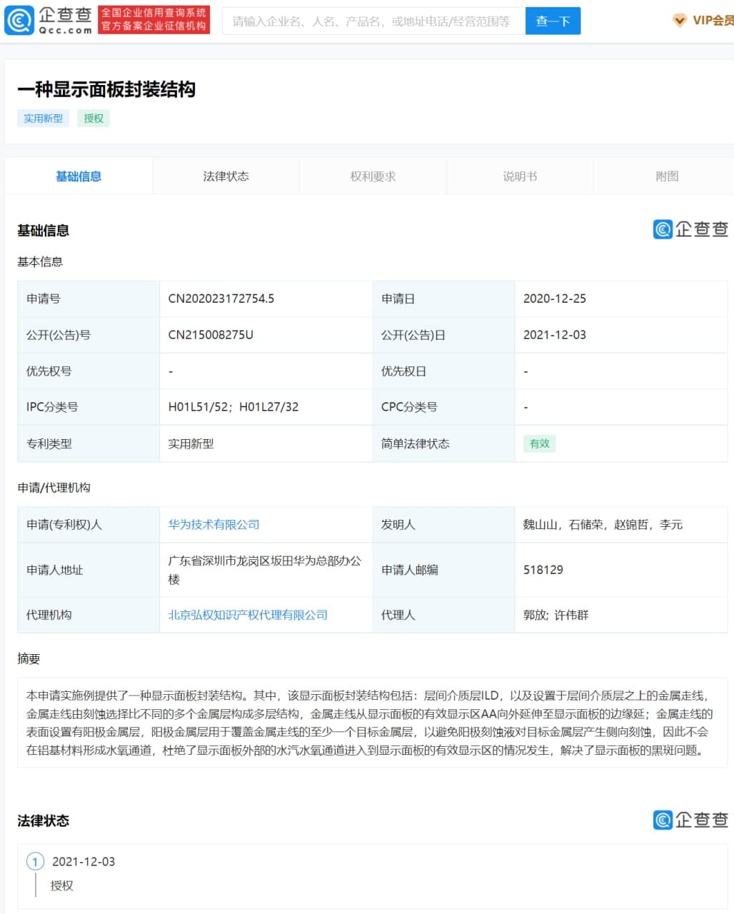
On December 3, 2021, Huawei has published a new patent for display panel packaging structure with announcement number CN215008275U in China. According to the information, the company applied for this patent on December 25, 2020, to the China Intellectual Property office.
The new Huawei patent technology provides a display panel packaging structure that resolves the problem of black spots encountered on display panels. Because display panel is the very costly part of any device as well as most useful. However, it is expensive to replace or repair it.

The patent application discloses that the display panel packaging structure includes: an interlayer dielectric layer ILD and metal traces arranged on the interlayer dielectric layer. The metal trace extends from the effective display area AA of the display panel to the edge of the display panel.
The surface of the metal trace is provided with an anode metal layer, and the anode metal layer is used to cover at least one target metal layer of the metal trace to avoid anode. The etching solution produces lateral etching on the target metal layer, so it does not form water and oxygen channels in the aluminum-based material.
It prevents the water vapor, water, and oxygen channels outside the display panel from entering the effective display area of the display panel and solves the problem of black spots on the display panel.
(Via)
The post Huawei innovated new packaging structure for display panel to solve black spot issue appeared first on Huawei Central.
Post a Comment
0 Comments